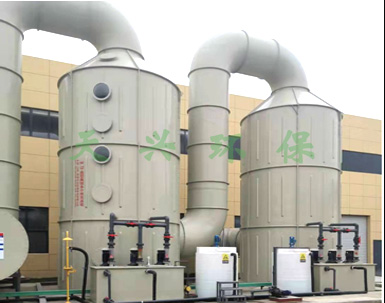
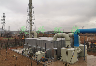
1. The tail gas of PECVD equipment mainly includes silane SiH 4 and ammonia NH 3 .
Treatment process: stainless steel combustion cylinder → stainless steel silane combustion scrubber → ammonia scrubber + centrifugal fan.
Main features: high removal rate of silane, high purification rate of ammonia and other water-soluble gases, small floor area, corrosion resistance and easy maintenance.
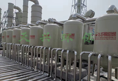
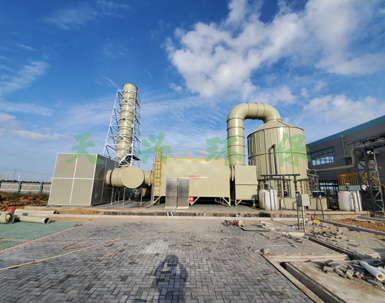
2. Screen printing waste gas process mainly involves the main equipment, printing press and sintering furnace. The waste gas produced is mainly organic waste gas and hot waste gas mainly composed of lipids and alcohols.
Treatment process: using activated carbon fiber adsorption tower.
Main features: the equipment covers a small area, corrosion resistance, easy mainten ance, no secondary pollution, purification efficiency is called activated carbon particles higher.

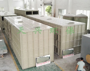
Shanxi Huaguang Electronics Co., Ltd

Jiangsu NANDA Optoelectronics

Suzhou Nengxun

Jiangsu Jingwang new energy

Xuzhou GCL

Kunshan flat panel display center

Tianjin China Airlines